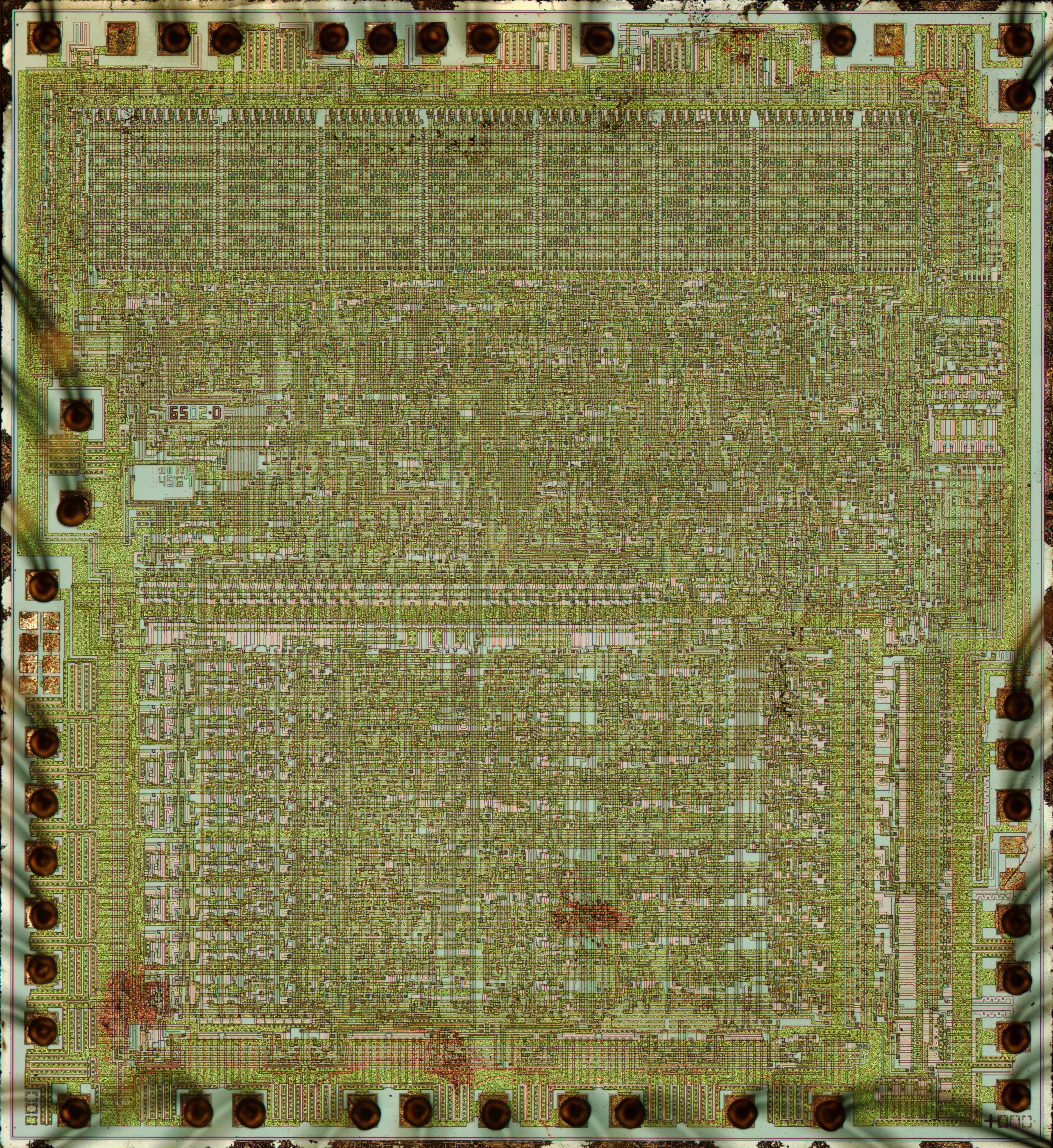
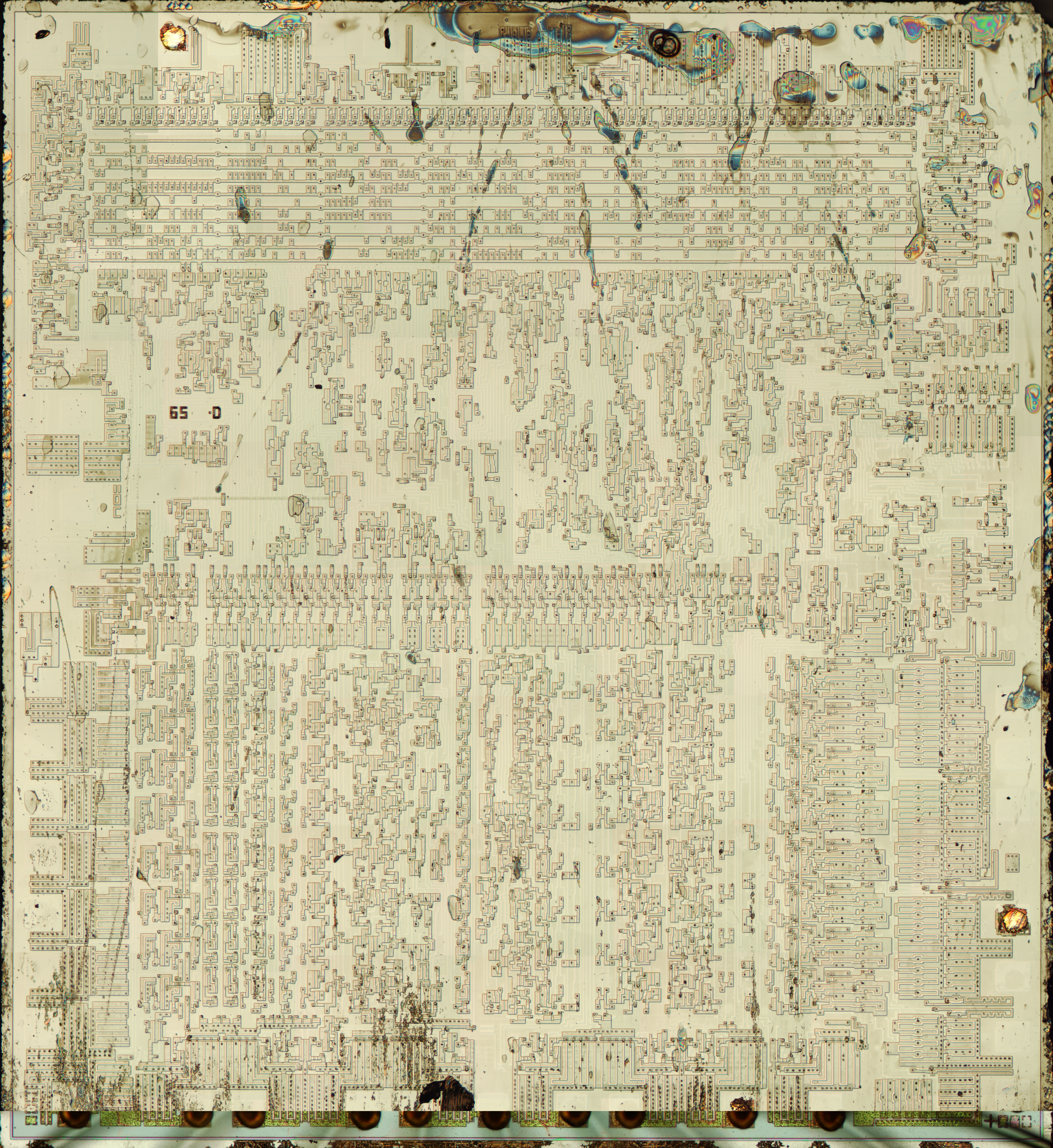
In the summer of 2009, the Visual6502.org project shot and assembled high resolution photographs of a MOS 6502 revision D. The surface of the chip was photographed, then the metal and polysilicon layers were stripped off to reveal the conductive substrate diffusion areas. The substrate was photographed, and the substrate image was aligned to the surface image. These two aligned images were then used to create the vector polygons that form the Visual6502 chip simulation.
Below are the aligned surface and substrate images, 4677 x 5097 pixels in size. The originals are twice the size in each direction, but those full size images were not used in the reconstruction. These were shot on a Nikon Optiphot 200 with 10x objective, and roughly 15x additional magnification going to the camera.
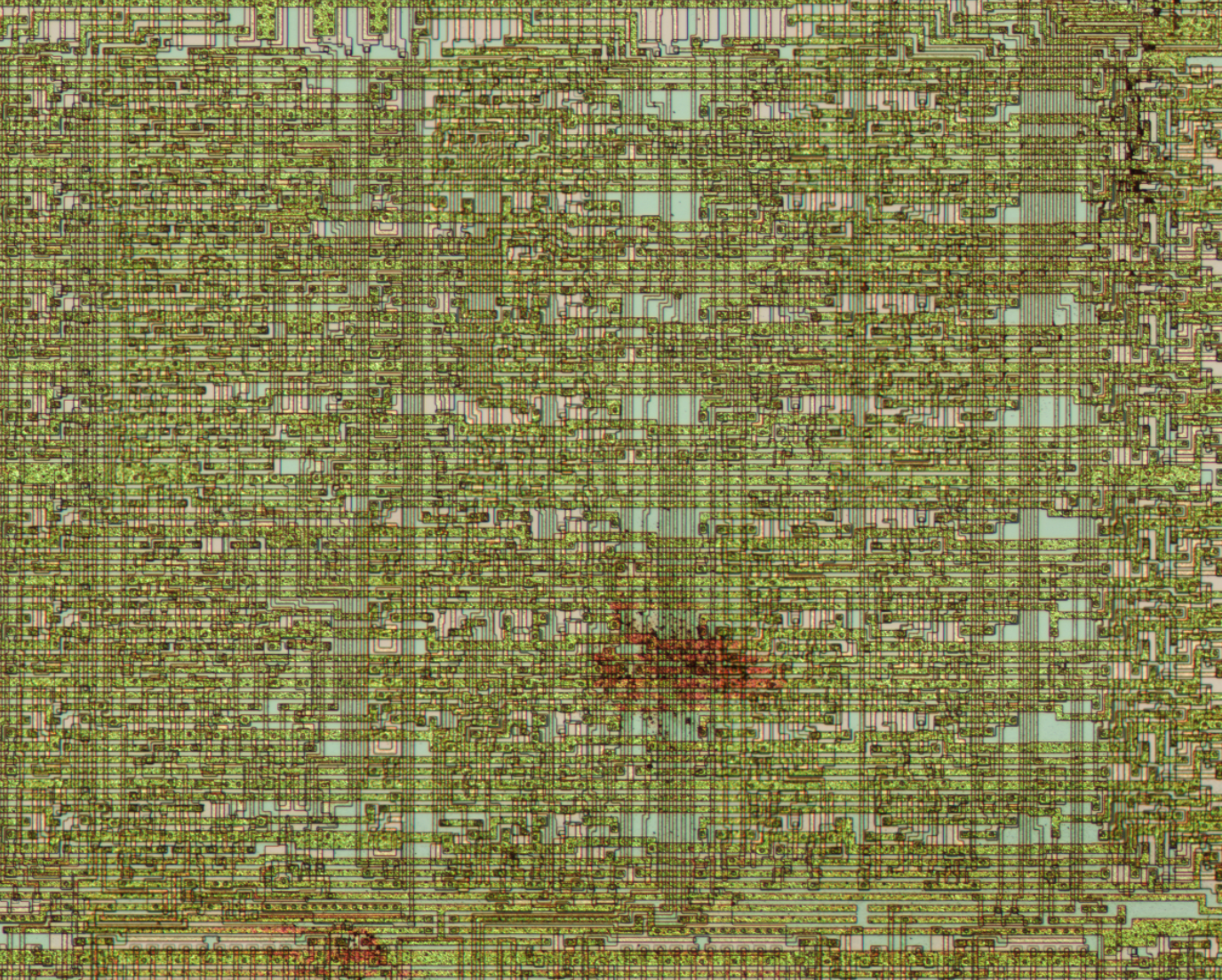
Register and ALU section, snapped from the interactive python app:
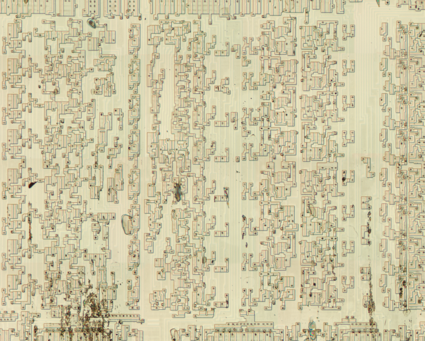
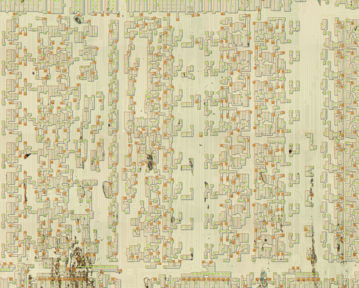
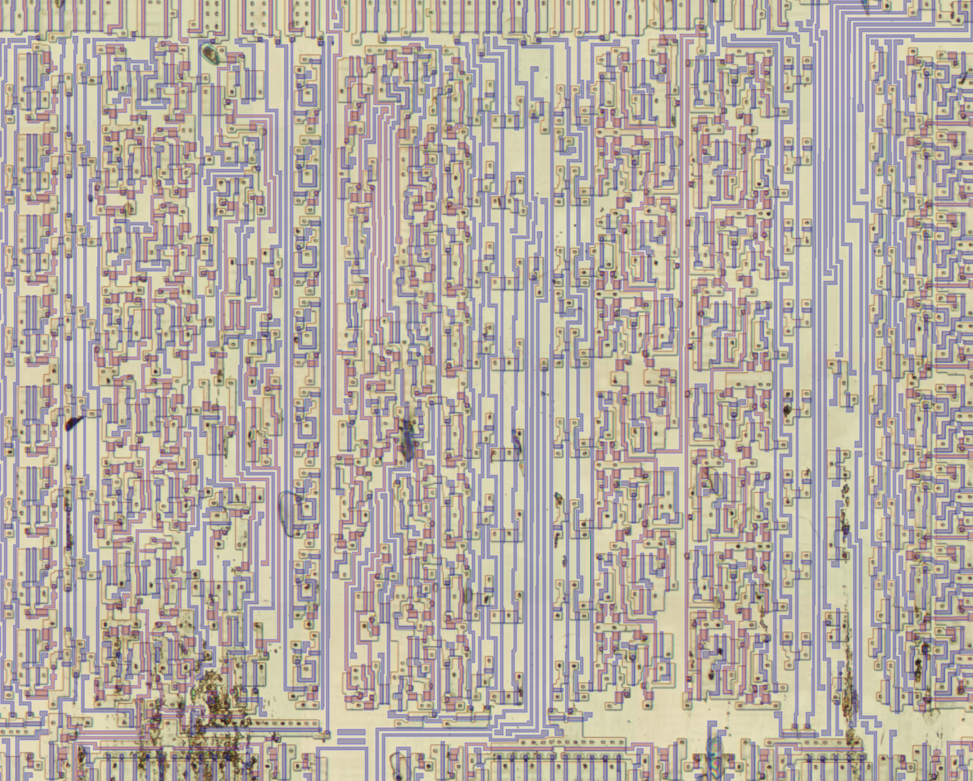
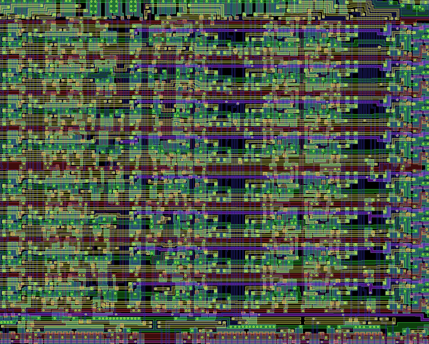
Aligned images of the chip and vector model with various layers by themselves or in combination with other layers:
MOS_6502_layers_all_metal.png
MOS_6502_layers_all_vec.png
MOS_6502_layers_all_vias.png
MOS_6502_layers_buried_contacts.png
MOS_6502_layers_clock_phases.png
MOS_6502_layers_diffusion.png
MOS_6502_layers_diffusion_and_common_metal.png
MOS_6502_layers_diffusion_buried_contacts.png
MOS_6502_layers_diffusion_vias.png
MOS_6502_layers_ground_metal_and_diffusion_vias.png
MOS_6502_layers_metal_for_ground_and_power.png
MOS_6502_layers_polysilicon.png
MOS_6502_layers_polysilicon_and_diffusion.png
MOS_6502_layers_polysilicon_vias.png
MOS_6502_layers_polysilicon_vias_buried_contacts.png
MOS_6502_layers_split_diffusion.png
MOS_6502_layers_substrate.png
MOS_6502_layers_top.png
MOS_6502_layers_vias_to_diffusion.png
MOS_6502_layers_vias_to_polysilicon.png